![]()
Golden Temple
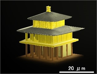
The micrograph is a Scanning Electron Microscope(SEM) image of a micron sized temple prepared with a
Focused Ion Beam(FIB) system.
In the FIB system, a micron-sized Silicon wafer was picked up with the micro-sampling method and
mounted on a needle stub of a specimen rotation holder. The posts were also fabricated using FIB by
rotating the specimen.
At 64th photo contest hosted by the Japanese Society of Microscopy in 2008.
Condition
Specimen: Single crystal Silicon
Instrument: Focused Ion & Electron Beam System nanoDUE'T NB5000
Magnification : ×2,000
Accelerating voltage: 5 kV
*All information related to these photographers is based on the information when the photo was taken.
*This work was presented at the "photo contest" hosted by the Japanese Society
of Microscopy.
*Reproduction or republication without permission prohibited.
*"nanoart" is registered trademark of Hitachi High-Tech Corporation in Japan.
Products & Services
Related Information

Hitachi High-Tech Social Media