Panorama Diffraction Pattern
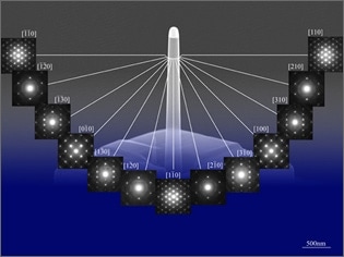
Here is the electron beam diffraction image observed with 180 degrees rounded. 13 electronic diffraction images centered in[110] are continually observed without lack. The center is an SEM image of the sample used for the observation. The sample was observed with sample rotation holder after processing to the diameter 0.2 µm column by FIB micro sampling method. Three-dimensional nanostructure analysis by an electron microscope can be said progressed.
1st Prize. At 61st photo contest hosted by the Japanese Society of Microscopy in 2005.
Condition
Specimen: Si mono crystal
Instrument: Transmission Electron Microscope H-9500
Accelerating voltage: 300 kV
Camera length: 0.5 m
*All information related to these photographers is based on the information when the photo was taken.
*This work was presented at the "photo contest" hosted by the Japanese Society
of Microscopy.
*Reproduction or republication without permission prohibited.
*"nanoart" is registered trademark of Hitachi High-Tech Corporation in Japan.
Products & Services
Related Information

Hitachi High-Tech Social Media